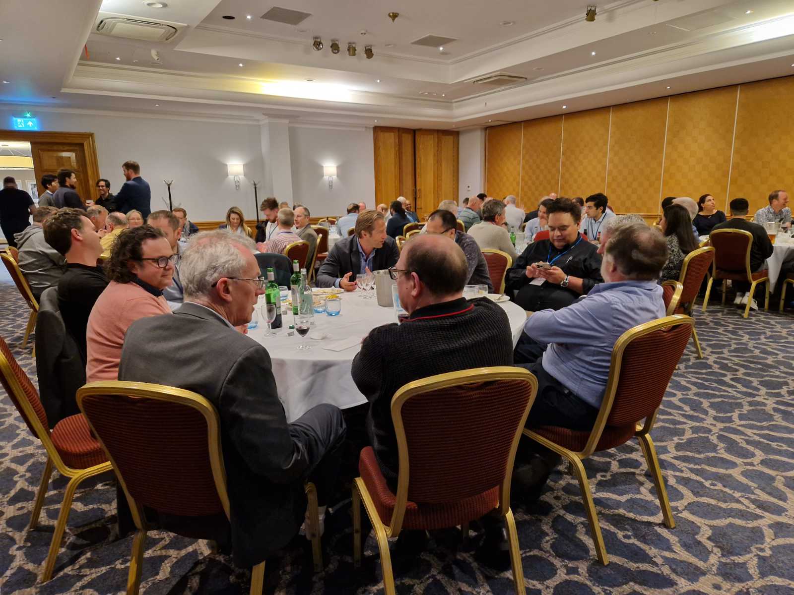
Young Engineer Sponsorship: The ARMMS RF & Microwave Society provides sponsorship for young engineers (28 or below) who have had papers accepted for presentation at each meeting. Sponsorship is £200 cash plus free attendance (including conference dinner and overnight accommodation). Potential candidates should identify themselves as eligible at time of submission and state their date of birth. This offer is limited to a maximum of 2 places per meeting. Richard Cavanagh of PRFI was sponsored to attend the April 2023 conference.
Best Paper Award: The Steve Evans-Pughe prize is awarded to the best presenter at each meeting. The prize is sponsored by Cadence. The winner of the April 2023 award was Moshen Khaili of Surrey University 6G Centre, the runner-up was Mahmoud Wagih of the University of Glasgow.
If you are interested in submitting a paper for presentation at this conference, please contact the technical coordinator (details below). Papers currently listed below are those already accepted. The deadline for submissions is 17th of March 2023. For exhibition enquiries please email exhibition@armms.org, for all other enquiries please email enquiries@armms.org
 |  |  |
Double Tree by Hilton Oxford Belfry
The Oxford Belfry
Nr Thame
OX9 2JW
| Web | https://www.theoxfordbelfry.co.uk |
Fatemeh Hoveizavi
3D EM and thermal simulation for RF system in package | |
| Fatemeh Hoveizavi | |
| EDRMEDESO | |
The design and optimization of high-performance RF systems and packages require accurate simulation models that can capture the behavior of the device under different operating conditions. This paper presents an approach that combines 3D electromagnetic (EM) simulation with High-Frequency Structure Simulator (HFSS) and thermal simulation with Icepacke to model the behavior of RF system in packages. The 3D EM simulation allows for accurate modeling of the device's electromagnetic behavior and the thermal simulation predicts the temperature distribution in the device and its package. The importance of 3D EM simulation is highlighted, as traditional 2D simulations are no longer sufficient to capture the full complexity of modern RF devices. By combining 3D EM simulation with thermal simulation, the proposed approach provides a more accurate representation of the device's behavior under different operating conditions. The proposed approach provides valuable insights for design engineers looking to optimize the performance of high-power and high-efficiency RF systems and packages for various applications. | |
| 3D EM and thermal simulation for RF system in package | |
A Practical Design Template for Doherty Amplifiers | |
| Derek Kozel | |
| Cardiff University | |
The Doherty architecture of RF Power Amplifiers has been studied extensively since its initial conception in 1936, however it remains challenging for a designer to identify and monitor the numerous interactions of passive and active components as a design moves from ideal concept to manufacturable circuit. This work identifies a set of observable properties specific to the Doherty architecture and presents measurement and display techniques to analyze them at all design stages. The approach is demonstrated by the design of an amplifier for 5G cellular signals on the 3.4 to 3.8 GHz band and achieving 45 Watts output and a power added efficiency of 54% at 8.5 dB backoff. | |
| A Practical Design Template for Doherty Amplifiers | |
Automated Measurement and Evaluation of 6-bit Amplitude and Phase Control Modules | |
| Richard Cavanagh | |
| PRFI | |
Vector modulators can be used in the design of phased array antennas and in feedforward linearization systems. This paper presents the automated testing of an S and C band 12-bit vector modulator, which uses a 6-bit phase shifter and 6-bit attenuator to vary signal phase and amplitude. A Python program was written to automate the testing of all 4096 possible states, to better understand the potential performance of the vector modulator. The combined performance is presented and is examined outside the respective frequency ranges of each device. This paper outlines the technical challenges faced in performing and processing the measurements and highlights the advantages of an automated test setup.
| |
| Automated Measurement and Evaluation of 6-bit Amplitude and Phase Control Modules | |
Conformable Single-Wire Transmission Lines: From Modelling to mmWave Applications | |
| Mahmoud Wagih | |
| University of Glasgow | |
The Gouabu single-wire transmission line (SWTL), guiding conformal surface waves offers a potential for reduced losses compared to two-conductor transmission lines, as well as free-space propagation. This presentation presents a state-of-the-art flexible single-wire transmission line with a coplanar waveguide feed. The line is implemented using conductive threads for on-body transmission, i.e. operation near a lossy medium, and is shown offering a >20 dB 0.5-4 GHz broadband link improvement over UWB antennas over the same range. In addition, the SWTL exhibits a stable group delay and enables conformable non-line-of-sight links. A shielded SWTL is then proposed for mmWave applications and is shown with 4x lower attenuation than a printed microstrip line on the same substrate at 50 GHz. To simplify the analysis of the line, a phase-accurate loss-less transmission line model is developed for the shielded line, showing an accurate group delay and under 7% phase error compared to measurements and full-wave simulations up to 50 GHz. The sensitivity of the SWTL to moisture and humidity is finally explored and compared to microstrip lines.
| |
| Conformable Single-Wire Transmission Lines: From Modelling to mmWave Applications | |
Design and Testing of an FR-4 based Reference PCB for use in Environmental Conditioning | |
| Lewis Manning | |
| NPL | |
A 4-layer Reference Printed Circuit Board (PCB) is designed that features RF structures and standards used to evaluate the performance before, during and after Environmental Conditioning. The design aims to emulate the operating environment of a sub-6 GHz PCB found in Industry and uses a popular FR-4 substrate throughout the PCB’s stack up (Isola 370 HR). S-Parameter Measurements of the reference PCB’s RF elements are performed to establish a performance benchmark prior to submission to Environmental Conditioning. These measurements are then evaluated against simulation data to determine how effective the design implementation is.
| |
| Design and Testing of an FR-4 based Reference PCB for use in Environmental Conditioning | |
Designing Calibration Standards for Cryogenic On-wafer S-parameter Measurements | |
| Sang-Hee Shin | |
| NPL | |
Microwave on-wafer measurement at cryogenic temperature plays an important role in the development of planar circuits for quantum computers. Such measurements enable direct characterisation of quantum circuits, without the need for additional components such as chip-to-PCB wire bonds, coaxial connectors, attenuators and cables. At NPL, we have developed a bespoke calibration substrate for cryogenic on-wafer measurements at temperatures down to 4 kelvin. High-resistivity silicon and niobium were used as the substrate and metallization material, respectively. The niobium metal layer is expected to be superconducting at 9 kelvin, making it an ideal choice of fabricating standards for use with our 4K cryogenic probe station. This paper describes the design process and preliminary study of the calibration substrate based on full-wave EM simulations using ANSYS High-Frequency Structure Simulator (HFSS). | |
| Designing Calibration Standards for Cryogenic On-wafer S-parameter Measurements | |
Evolution of the Wafer-level Characterization Solutions: Towards mmW 6G Applications | |
| Vince Mallette, Andrej Rumiantsev | |
| MPI Corporation | |
In this presentation, we will briefly review the evolution of mmWave instrumentation and how it enabled complex characterization tasks at the wafer-level. We will look into the challenges and drivers of the 6G applied research and related technologies, such as instrumentation versatility, probe system integration complexity, broadband RF probes, calibration solutions, and metrology aspects. We will discuss possible system integration solutions and present selected measurement results for broadband single-ended and differential characterization. | |
| Evolution of the Wafer-level Characterization Solutions: Towards mmW 6G Applications | |
Investigation of Radiation Gain Enhancement Techniques for Microstrip | |
| Michael F. Adamson | |
| Cranfield University | |
It is well known that patch antenna radiation can be increased via the integration of a combination of dielectric and/or ferrite supersaturates or planar sheets. Previously researchers [1] have employed full-wave analysis methods to design and optimise the material choice, thickness and separation in these complicated structures. This approach is unwieldy, providing limited understanding and often leads to time consuming redesign if material layers are changed. Here we describe the development of an equivalent transmission line model that includes the patch antenna, or array, the radiation model for an arbitrary dielectric/ferrite cascaded structure. The model enables rapid evaluation and understanding of the various effects that material selection and layer spacing have on the resultant radiated field pattern and impedance bandwidth of the radiating system.
| |
| Investigation of Radiation Gain Enhancement Techniques for Microstrip | |
Milimeter-wave load-pull measurment of GaN HEMT: driving the next generation of advanced power amplifiers | |
| Roberto Quaglia | |
| University of Cardiff | |
Power Amplifiers (PAs) remain a crucial component in the high frequency front-end of all wireless systems. The increased interest in millimetre-wave frequency bands for a variety of applications posing more new challenges to device manufacturers and circuit designers. GaN HEMTs can help addressing some of these challenges as they lead to high power PAs with better efficiency compared to other technologies. The UK has a rich habitat in the microwave sector; from small design houses to large multinationals providing PA design services and products, and there are increasing investments to try and establish a sovereign source of GaN HEMT technology. The success of this venture heavily depends on the availability of experimental characterisation capabilities, with load pull being the ultimate tool in this context for supporting both the foundries, with detailed information on the devices being developed, and the designers, by supporting accurate large-signal modelling. Cardiff University and the CSA Catapult have a comprehensive provision of load-pull characterisation options. This paper will discuss three of the measurement systems available, all capable of harmonic load pull and pulsed RF and bias, with passive implementations up to 110 GHz, and active up to 67 GHz, through three measurement campaigns on different GaN technologies supporting advanced PA design (harmonically tuned, Doherty) for up- and down-link satellite frequencies.
| |
| Milimeter-wave load-pull measurment of GaN HEMT: driving the next generation of advanced power amplifiers | |
Millimetre-wave front-end antennas based on antenna-in-packaging (AiP) technology | |
| YI Wang | |
| University of Birmingham | |
This talk will present our recent work on millimetre-wave front-end antennas using antenna-in-packaging (AiP) technology. Stack-ups up to 14 layers have been implemented using high-density-interconnect (HDI) technology. Dual-polarisation antennas have been designed aiming for large scanning angles of 60 deg. Method to ensure isolation at the high angle will be discussed. Some measurement results of the antennas will be shown. The antennas are designed to integrate with commercial RFICs. The considerations in interconnection and thermal modelling will be discussed. | |
Reconfigurable intelligent surfaces for 5G and 6G coverage enhancement | |
| Mohsen Khalily | |
| Surrey university 6G center | |
Traditionally, all the dynamic and adaptive features of a typical mobile network are controlled either by the base station or the user equipment, while the wireless propagation environment remains unaware of various communications processes going through it. The existing mobile network operators face a significant challenge of not only ensuring seamless connectivity in harsh propagation environments but of supporting an ever-increasing number of mobile users, which sometimes, are unevenly distributed in a network. Reconfigurable Intelligent Surface (RISs) are a promising technology that can address the aforementioned challenges by sensing the environment, recycling the existing radio waves and enabling non-line-of-sight (NLoS) communications. RIS can achieve this by manipulating those electromagnetic (EM) waves which are impinging on it and redirect them to the desired angle with a relatively low power consumption. At 6GIC, University of Surrey we have developed world's first reflective and transmissive metasurface for O2O, I2I, and O2I coverage enhancement. In this paper we summarise our achievements in terms of RIS design, prototyping and research challenges. | |
| Reconfigurable intelligent surfaces for 5G and 6G coverage enhancement | |
Simulating Process Variation Impact on the Performance of a mm-Wave Patch Array Antenna | |
| Priya Shinghal | |
| Keysight | |
Millimeter-wave structures and circuits are susceptible to performance degradation due to fabrication tolerances. To avoid multiple fabrication iterations due to such unaccounted effects, it becomes imperative that the impact of process variations is taken into consideration during the design and simulation phase. This paper presents the use case of an E-Band microstrip patch antenna array’s design, along with its simulation and measurement results, to demonstrate this scenario. This 4×4 antenna array was designed to operate in the 76-77 GHz frequency band and has a simulated -10 dB impedance bandwidth of around 2.4 GHz. As commonly seen with millimeter-wave designs, the post fabrication S11 measurements of this antenna showed a noticeable shift in its frequency response as compared to the simulated results. Here, Keysight’s ADS RFPro full 3D EM simulation software was utilized to effectively predict the impact of manufacturing tolerances on the desired performance of the antenna. Parametric process variation simulations in RFPro revealed that there was an under-etching of copper on the printed circuit board during fabrication. This potentially resulted in changes to the physical dimensions of the individual radiating patches, thereby resulting in a downward shift of the resonant frequency. These simulation results are further validated by means of measurements.
| |
| Simulating Process Variation Impact on the Performance of a mm-Wave Patch Array Antenna | |
The Challenges of NTN Testing | |
| Guy Purchon | |
| Viavi Solutions | |
3GPP 5G Release 17 has introduced a new mode of deploying networks: Non Terrestrial Networks based on a constellation of Low Earth Orbiting Satellites. What are the RF challenges when the mobile has to connect with a basestation orbiting several hundred kms overhead? This paper looks at how 3GPP has adapted the basestation to mobile link architecture and what are the implications and difficulties for the RF link in both directions.
| |
| The Challenges of NTN Testing | |
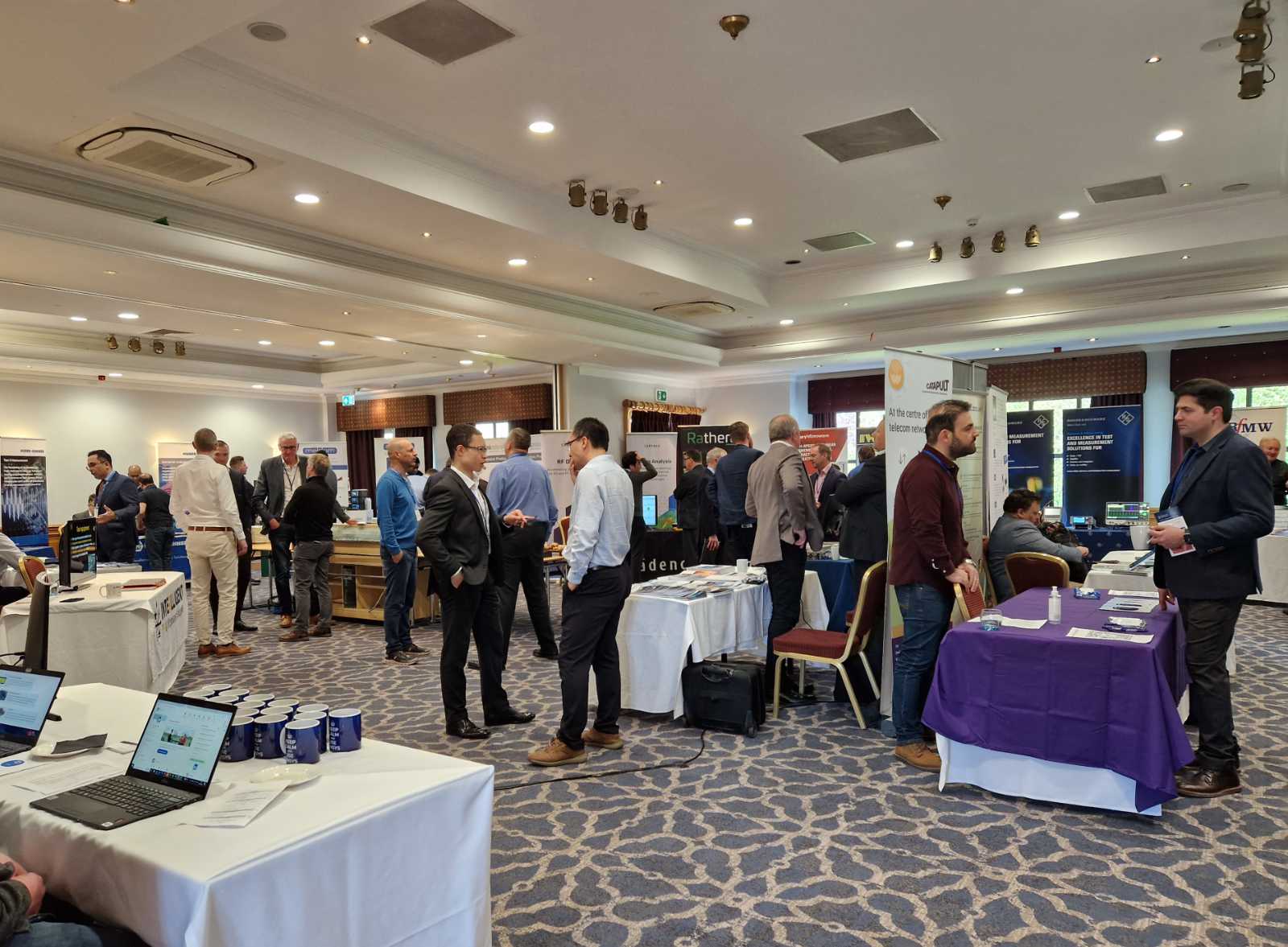
Companies booking two or more delegate places are able to take part in the commercial exhibition that accompanies the conference. Please note: there is a maximum of 20 exhibition tables at each meeting, these are offered on a first come basis. Booking two delegate places does not guarantee an exhibition space, please email exhibition@armms.org to check availability and reserve and exhibition space.
The society would like to thank JFW for sponsoring the April 2023 meeting.
Contributions are invited with an emphasis on RF and microwave design, research, testing and associated subjects. An oral presentation will be made at the meeting and a written paper will be required for publication in the society digest, which is distributed to delegates at the meeting. Prospective speakers are requested to submit a title and a short abstract to the technical coordinator (see above) as soon as possible.
Click here to view our Guidelines for Authors
Click here to view our Publication Release Form